I’m writing this because even though it’s already 2020, this kind of stuff still cannot be found anywhere in the internet!
Stacking layers of materials is something we all do in so many engineering applications! Electronic components, batteries, constructions panels, ovens, refrigerators and so many other layered materials that are inevitably under heat transfer. We want to predict the temperatures on the stack, at all layers, to ensure the materials are going to withstand the transfer of heat. In order to do that, any engineer worth their salt will already have used the Thermal/Electrical Circuit Analogy. And it works wonders!
But what if we want to do transient analyses? What if the materials are going to be stressed by some quick burst of power; or some sequence of bursts at a certain frequency? Of course, we can always just do some FEM and solve our issue – but one might find that this can become a multi-scale problem if there’s low frequencies AND high frequencies involved.
This is commonly the case in semiconductors. Applications I’m familiar with are related to LED pulsing, but I’m sure one will find many others. Another more obscure application I found in my research has to do with unsteady measurements of surface temperature when fluid is flowing on a surface. Some frequencies will be too fast and the stack of materials will not respond, so how do we proceed in that scenario? How to predict the temperature rises and – more importantly – understand what we need to change in the design in order to improve its frequency response?
Well, it turns out we can extend the thermal circuit analogy to transients by including the component’s thermal capacitance. Most layers in a stack would then be easily lumped into RC low-pass filters. This is the “basic approach” and it works – to a point.
So let’s examine it, to understand its pros and also its limitations:
The thermal capacitor
Capacitance in electrical circuits is the ability of a given electrical component to store charge. In the thermal analogy, this “charge” is heat – and the thermal capacitance is just the mass of the component times its heat capacity (

Which means that, for a given heat flow 


The terms 

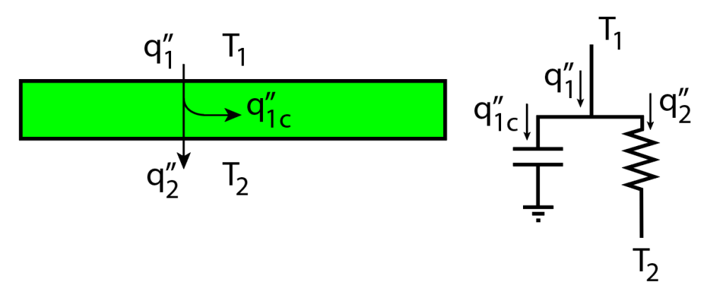
Obviously, this single-layer model is rather simple and does not constitute of much of an issue. The RC circuit has a time constant, 


It is really worth observing, though, that the capacitor is not connected to 

Stacking them up (plus all the ways you will mess this up)
For thermal stacks, it is not straightforward how to assemble the circuits together. Do we put the RC circuits in series with each other? As it turns out – not really. To understand why, let’s think about what happens in a two-layer stack:
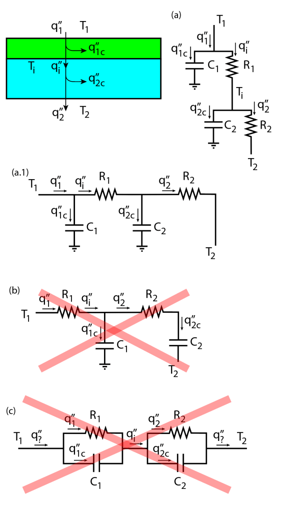
Looking at the picture above, we have a stack of two layers and 3 different circuits that could (potentially) represent it. The circuit (a) represents how we would construct the thermal RC network using the same strategy as for the single layer explained before. (a.1) is simply another representation of the same circuit, perhaps less “bulky”. The circuits (b) and (c) are wrong because they do not represent the thermal equations that describe the stack. Let’s see why:
The first layer of the stack has an input heat flux of 


This sounds easy because you already have the answer spoon-fed to you. But if you were left to your devices, I would bet many of you (including past me) would come up with the circuit representations (b) and (c). (b) doesn’t make any sense because capacitors block DC, therefore there would be no DC heat flux through the stack – total non-sense!
The circuit in (c) also does not make sense, but it is not clear why at a first glance. If you follow Kirchoff’s laws, however, you will see that (c) cannot be right, because in the node at 
It is not really very intuitive that the capacitor of the first layer of the stack should be connected to ground, instead of
We can also solve the full heat pde with circuits!
Ok, so we tackled the single wall and the stacked double-wall problem. I think having gone through how this can go wrong, you can now build this to multi-walled systems easily. As you probably already realized, each new layer will behave as a new first-order system, and some very interesting behavior can appear as extra poles are introduced by the new layers. One thing, however, that is worth noting, is that this approach completely fails at high enough frequencies.
To understand why, let’s think about it a little further. If the temperature oscillations in 
But the problem in the (zero-dimensional) lumped element model is that the whole element’s temperature is assumed to be a constant value. At high enough frequencies, this won’t be the case anymore. We can see why the lumped element model becomes inaccurate by modeling the standard 1D heat equation over a slab:


The negative sign in the left-hand side is related to the direction of the coordinate system. One can recover the same equations by distributing the lumped element model related to each layer into the following circuit:
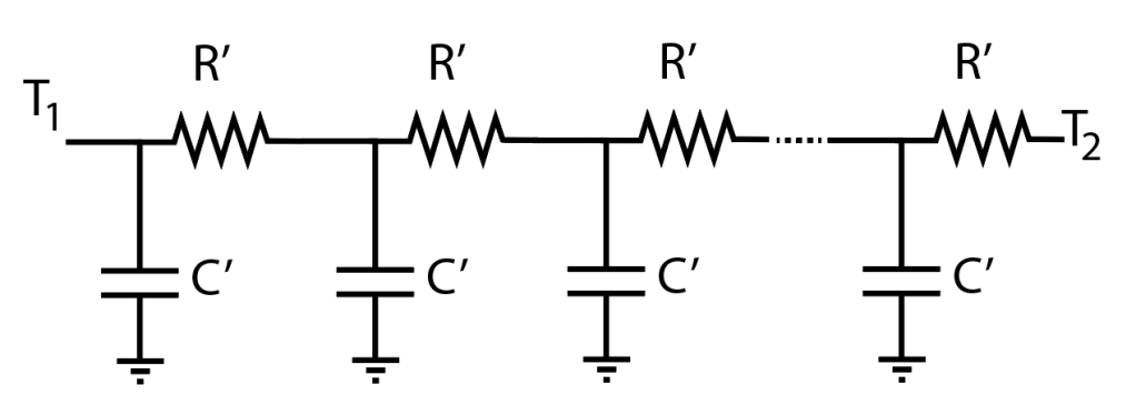
Where 

A thermal layer is actually a transmission line
I invite you to read the article on Wikipedia about transmission lines if you’re not familiar with this concept, or read the book “Time-Harmonic Electromagnetic Fields”, by Harrington, 1961. Transmission line is an electrical model for pairs of conductors at high frequencies. At high enough frequencies, the pair of conductor’s distributed capacitance and inductance creates waves inside the conductor, which can be modeled by the wave equation. The element of the electrical transmission line is displayed below (figure from the Wikipedia article):
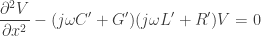
The electrical transmission line follows the 1-dimensional damped wave equation, which is derived from the Telegrapher’s equations:


We can easily see this is the wave equation by taking the Fourier Transform of the two equations:


And then replacing, say, the 


Taking the IFT:

Which, obviously, is the wave equation. It’s damped by the distributed resistance 


Where the thermal diffusivity is 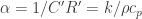
how this interpretation can be useful
Ok, by now you might be finding this all quite trivial and, perhaps, an over-complication of the heat transfer problem. Why would one need to invoke the far more complex “transmission line” to describe the behavior of such a simple system? Well, it basically allows us to easily determine the temperature transfer functions at different points in the stack (perhaps, easily is not the best word, but with a couple easily-programmable equations), without having to solve the differential equations numerically. Plus, it allows us a very cool insight about the behavior of the themal stack at higher frequencies. As it turns out, at high enough frequencies the first layer’s characteristic impedance – a material property – dominates the transfer function.
Thermal transmission lines in practice: the pulsed led
Let’s first analyze the following case that I find is the most practical for high frequency thermal stacks: An electronic power dissipation device that sources power in short bursts. I mentioned in a previous post that you can massively overdrive LEDs to produce a lot more light than “designed” for short bursts, which enables one to expose high speed cameras – like a camera flash. We’ll look at the Luminus Devices Phlatlight CBT-140 for this analysis. The reason why AC thermal analysis is important in pulsed LEDs is because, even though the mean temperatures of each component might be within spec due to the high thermal capacitance of the heat sink, the power burst will temporarily increase the temperature of the LED die, and we obviously also don’t want that to exceed the specs of the LED. Concerns about thermal expansion will not be addressed in this discussion – but you should also do your research on that!
The CBT-140 die looks like shown below. The named squares in the electrical analogy (bottom right) represent the “transmission lines” for each component.
We will consider the die is made of sapphire (many high power LED dies are made of it). This might be incorrect for this model – but I could not find any specs on that. The die has 0.31mm thickness; whereas the copper has 3.44mm thickness. The aluminium heat sink is pretty large. For the sake of this analysis we’ll consider 10mm. As we’ll detail later – it won’t matter much for the AC analysis.
So what we want to find is the “input impedance” as seen by the current source just above the die in the figure. The current source is a heat flux source, which in this case would be a square wave with some (low) duty cycle, since power is generated by the (micrometer thin) LED just above the sapphire die. Because there’s a cascade of 3 “coupled transmission lines”, we have to use the transmission line input impedance formula three times. From Wikipedia:

Where 


Note the characteristic impedance is inversely proportional to the square root of the frequency. This will explain the “half-order” decay (-10dB/decade) behavior in the frequency domain we’ll see later (in contrast with a first-order expected from these RC networks). The square root of 


As we discussed, the math is not the “prettiest”, but this can all easily be hidden behind an Excel or Matlab formula. In this case, using the properties of the three materials shown in the table below and a convection coefficient of 
| Aluminium 6061 | Copper | Sapphire | |
|---|---|---|---|
 | 180 W/m K | 287 W/m K | 34.6 W/m K |
 | 1256 J/Kg K | 376 J/Kg K | 648 J/Kg K |
 | 2710 Kg/m3 | 8800 Kg/m3 | 3930 Kg/m3 |
|  |  |  |
|  |  |  |
In order to find the “input impedance” at the node 


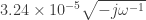
In this case we are driving the LED with a 500 nanosecond square pulse that repeats at 100 kHz. The drive current of the LED is 200A, and given the die area of 14 mm2 and a voltage drop of 20V in the LED, we have an instantaneous power of 285 MW/m2. That’s a lot of power!! Well, as it turns out, the mean flux of power (in this case, at a duty cycle of 5%, 14.2 MW/m2) appears in the spectrum at the DC component, but the sharp bursts of power also generate incredibly high amounts of high frequency power flux that really need to be considered.
Looking at the figure above, the solid, thick black line is the actual frequency transfer function of the whole thermal stack. The dashed blue line represents the lumped element assumption and it is a good model until about a frequency of 0.05 Hz. It then starts to fail when the aluminium starts to kill the waves very close to its surface due to its “large characteristc impedance”, 
This issue happens once again for the copper (not clear exactly where) and then finally for the die itself (the sapphire) above the frequency of 40 Hz. Then the characteristic impedance of the sapphire dominates the transfer function – i.e., the sapphire is thick enough to be effectively “infinite”, as far as high frequency heat transfer is concerned (the sapphire is 0.31mm thick!!). The temperature waves then decay inside the sapphire, and very little oscillations can be detected at its opposite side. At those frequencies, it doesn’t matter anymore which material you put at the interface. It will not see any temperature oscillations.
All of this insight we get without needing to numerically solve the heat equation is quite fascinating. We now know that at high frequencies, the dominant part of the frequency response is a material property – meaning that a material choice here is crucial for high frequency heat transfer!
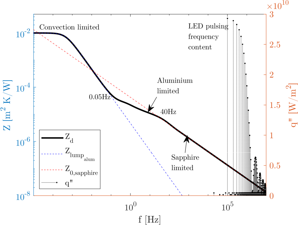
How important? Well, let’s run the numbers and see what the wave looks like. I removed the DC part of the wave, because this LED really needs some thermal mass attached to it (the aluminium block) as no amount of convection or heat-sinking will get rid of this insane amount of power. Therefore, let’s only focus on the oscillatory part of the wave:
We can see that we predict an overtemperature of almost 25 K for the die surface for this case. This is on top of the die heating up from the constant heat flux at DC. It is quite a lot and could (in fact, DOES) easily lead to die failure if one only reads the copper temperature. Therefore, one needs to account for this overtemperature when designing an emergency shutoff system – otherwise, it’ll only think about shutting off 25 degrees after the LED failed!
Temperature sensitive paint – high frequency measurements
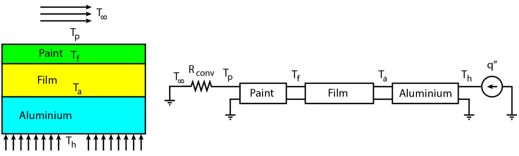
So this one is quite an interesting application from the research standpoint! We use temperature sensitive paints to perform measurements in aerodynamic models. We paint an aerodynamic surface with this special paint, and it fluoresces under UV illumination, emitting a strong (usually red) light signal at colder temperatures and a weaker signal as the paint surface becomes hotter. An example of supplier of these paints is given here. Though this is quite a specialized application used mostly in high end aerodynamics research, there’s still a lot of interest into understanding its behavior.
So let’s say we want to perform unsteady measurements of heat transfer coefficient at the surface. We put the surface under a flow of nominally known temperature (for this example, a jet impinging on a surface) and then we use the TSP technique to image the temperature map over the impinging surface; getting a full temperature map. As the flow oscillates, we have fluctuations of this convection coefficient – which translate to measured fluctuations in temperature. Obviously, we might not be able to see them if the temperature does not fluctuate much because the substrate of the surface has too much thermal capacitance (as discussed throughout this article). In fact, now we know we have waves of temperature going through the material, which will be rapidly decaying. It might perhaps be the case that the waves are so weak that we cannot detect them. Therefore, we need to assess whether we can measure these waves by comparing the expected signal generated by the oscillations with the dynamic range of our camera.
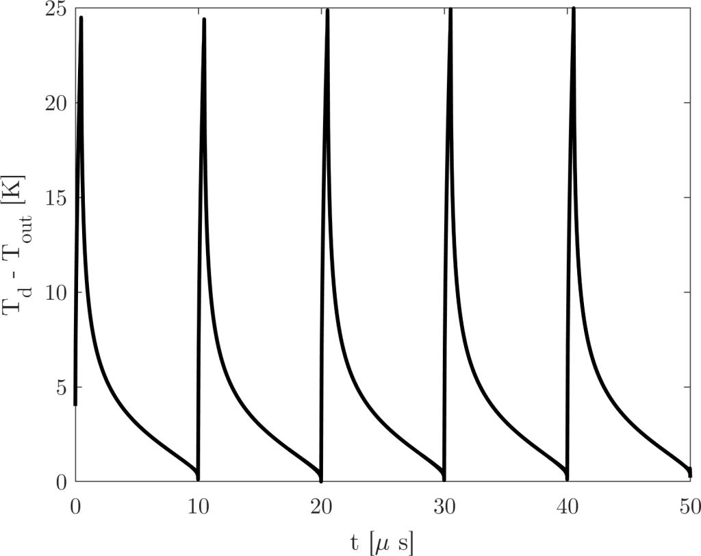
Let’s start with a rather simplistic setup – to illustrate the issue. Say we have an impinging jet as in the figure below. The impinging jet is the flowing arrows at 
A “thin” layer of temperature sensitive paint is painted on top of a 10mm thick aluminium plate. The layer of paint, although thin, will have an effect on the transfer function. Here’s what happens as we change the paint thickness. The solid black line represents a reasonable paint thickness (5 microns).
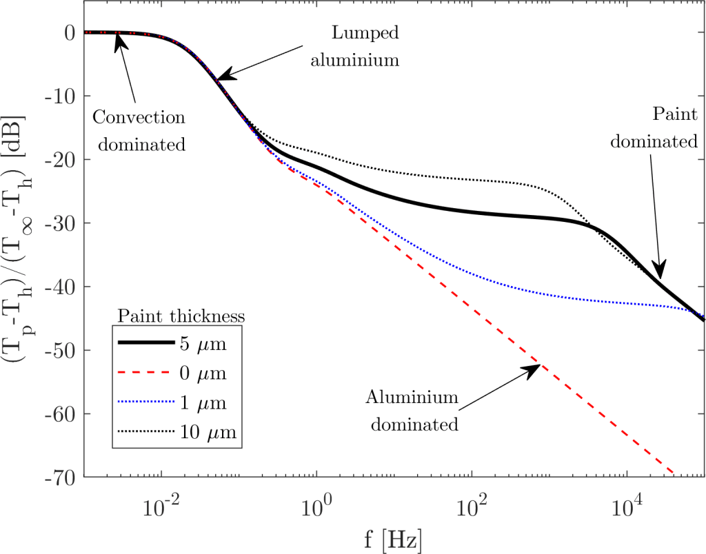
As we can see, the transfer function is highly dependent on the thickness of the paint: If the paint is too thin, we get dominance of the aluminium block on the transfer function, which reduces the signal gain very significantly at higher frequencies. As the paint layer thickens, it starts dominating the transfer function – but knowing the paint thickness might be a challenge.
A solution to this issue is to use an insulating film of similar properties to the paint binder (in this case, the binder used for the calculations was a Polyacrylic Acid polymer). Most importantly, if the two materials have similar characteristic impedances
Polyacrylic acid has the following thermal properties (sources here and here). The film considered here is a PET film (this one).
| Polyacrylic acid | PET Film | |
|---|---|---|
| 0.543 W/m K | 0.21 W/m K |
| 1248 J/Kg K | 1465 J/Kg K |
| 1440 Kg/m3 | 1170 Kg/m3 |
|  |  |
|  |  |
As we can see, the thermal impedance of the two materials is somewhat similar. This means less reflection will occur at the interface; which will help with a reduced dependence of the transfer function on the paint coat thickness. The circuit analyzed becomes the following:
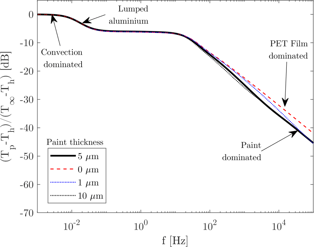
This graph shows a great improvement; because the transfer function at higher frequencies is less dependent in the paint thickness. Not perfect – this would only be possible with a perfect match of thermal impedances. Nevertheless, this can definitely be used to make some measurements.
As a remark – the frequencies of interest in this work are around 20 kHz. The gain is then about -38dB (5 microns paint thickness); which is defined as ![20 \log_{10}[(T_p-T_h)/(T_\infty -T_h)]](https://s0.wp.com/latex.php?latex=20+%5Clog_%7B10%7D%5B%28T_p-T_h%29%2F%28T_%5Cinfty+-T_h%29%5D&bg=ffffff&fg=333333&s=0&c=20201002)


I’ll post updates as we perform experiments!
Tying it all back to the fourier number
So we see this interesting transfer function that switches between the lumped RC circuit assumption (with a -20dB/decade decay) to the continuous transmission line (with a -10dB/decade decay). Why does that happen and where is the “kink” in the graph?
Well, we’ll see this ties back to the thermal theory; once we find the kink frequency: The kink is where the -20dB/decade and the -10dB/decade cross. At the -20dB/decade regime, a slab of material has behaves as a capacitor and its thermal impedance is:

We have the definition of 

The kink is located about where 


This gives us the radian frequency of the kink:

Now you should already be recognizing that we have an interesting non-dimensional coming up, as 

The non-dimensional is; obviously; the Fourier number:

We usually see the Fourier number with a time in the numerator 
I boxed the 
